admin
Semiconductor Industry Value Chain: Bottlenecks, Margins, and Market Outlook
When investors think about the microchip boom, attention almost always gravitates toward headline chip designers like NVIDIA, AMD, or Apple. Yet focusing exclusively on the companies whose logos appear on finished processors overlooks how modern silicon is actually built—and where the widest economic moats reside.
In the first half of 2026 alone, global semiconductor sales surged 102% year-over-year to $702 billion, putting the full-year market on track to reach roughly $1.655 trillion “. Fueling that expansion is an intricate, nine-stage semiconductor industry value chain spanning specialized software, ultra-pure materials, precision lithography, contract foundries, and advanced packaging.
Understanding how value flows across these nine stages reveals why a handful of specialized suppliers command monopoly-like pricing power, recurring consumable revenues, and gross margins exceeding 70%. For investors and industry analysts, mapping these chokepoints is essential to identifying durable compounders while avoiding cyclical traps.
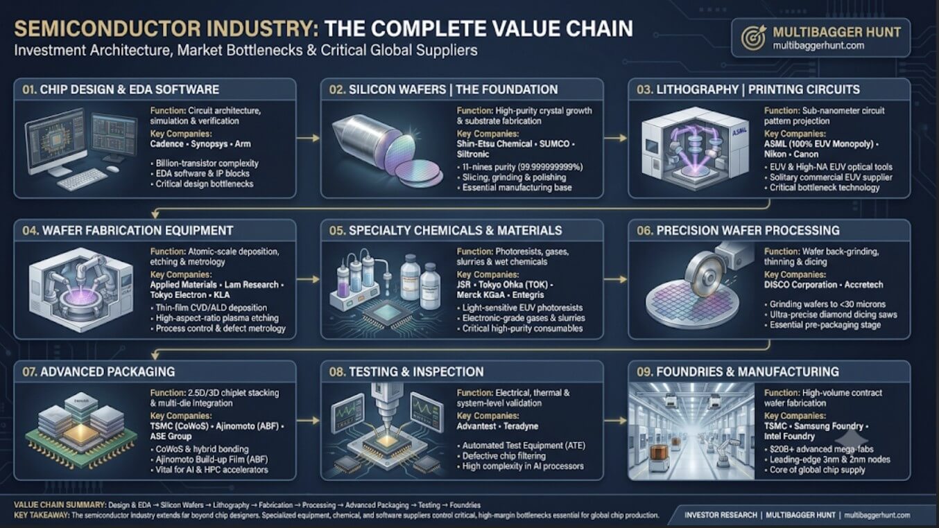
End-to-End Semiconductor Industry Value Chain Overview
Before examining each segment in detail, it helps to view the entire production pipeline as a sequential chain of dependencies. A delay or yield loss at any single link prevents finished chips from reaching data centers, smartphones, or autonomous vehicles.
Production Flow: Chip Design (EDA) → Silicon Wafers → Lithography → Wafer Fabrication → Precision Dicing → Advanced Packaging → Final Testing → Foundry Integration
| Value Chain Stage | Core Function | Dominant Leaders | Primary Moat Driver |
| 1. Chip Design & EDA | Circuit architecture, simulation, and IP blocks | Cadence, Synopsys | High switching costs and R&D lock-in |
| 2. Silicon Wafers | Ultra-pure crystalline semiconductor substrates | Shin-Etsu Chemical, SUMCO | Crystal-growth yield and multi-year contracts |
| 3. Lithography | Printing nanometer-scale circuit patterns | ASML | Sole commercial EUV and High-NA EUV supplier |
| 4. Wafer Fab Equipment | Deposition, etching, planarization, and metrology | Applied Materials, Lam Research, TEL, KLA | Atomic-scale process control and installed base |
| 5. Specialty Materials | Photoresists, wet chemicals, gases, and slurries | JSR, Tokyo Ohka, Merck, Entegris | Qualification barriers and recurring wafer usage |
| 6. Precision Processing | Ultra-thin wafer grinding, dicing, and polishing | DISCO Corporation | Micron-level mechanical precision and consumables |
| 7. Advanced Packaging | Multi-die integration, interposers, and substrates | TSMC (CoWoS), Ajinomoto, ASE | Thermal/interconnect density and capacity limits |
| 8. Testing & Inspection | Electrical, thermal, and system-level validation | Advantest, Teradyne | Custom test-head software and AI chip complexity |
| 9. Foundries | High-volume contract wafer fabrication | TSMC, Samsung Foundry, Intel Foundry | Capital scale ($30B+ fabs) and process yield |
To understand how these segments interact with broader data center spending, see our breakdown of AI infrastructure capital expenditure trends.
1. Chip Design & Electronic Design Automation (EDA) Software
Every semiconductor begins as lines of code rather than physical silicon. Modern artificial intelligence accelerators pack more than 100 billion transistors onto a single die, making manual circuit layout physically impossible.
Electronic Design Automation (EDA) software provides the digital workbench engineers use to design, simulate, verify, and test chip architectures before a single wafer enters a fabrication plant.
- The Duopoly Advantage: Cadence Design Systems and Synopsys control the vast majority of the global EDA market. Both companies also license pre-verified semiconductor intellectual property (IP) blocks—such as PCIe interfaces, memory controllers, and processor cores—that accelerate time-to-market for fabless chipmakers.
- AI-Driven Complexity: As chipmakers transition to gate-all-around (GAA) transistor architectures and multi-die chiplets, verification workloads grow exponentially. Both Cadence and Synopsys have embedded generative AI into their design suites to automate floorplanning and power optimization, allowing them to raise average selling prices upon contract renewal.
- Financial Profile: Unlike hardware suppliers whose sales fluctuate with factory construction, EDA vendors operate on multi-year, time-based software licenses. This generates predictable recurring revenue, gross margins consistently above 80%, and resilient cash flow even during semiconductor downturns.
2. Silicon Wafers: The Physical Foundation
Once a chip design is finalized (“taped out”), manufacturing begins on circular discs of ultra-pure crystalline silicon known as wafers. Leading-edge logic and memory fabs rely almost exclusively on 300-millimeter (12-inch) wafers.
Producing semiconductor-grade silicon requires refining raw metallurgical silicon to “eleven nines” purity (99.999999999% pure)—meaning fewer than one impurity atom per hundred billion silicon atoms.
- Oligopoly Market Structure: Japanese chemical giants Shin-Etsu Chemical and SUMCO collectively command over half of the global 300mm silicon wafer supply, alongside Siltronic, GlobalWafers, and SK Siltron.
- Manufacturing Rigor: Ingots of single-crystal silicon are grown using the Czochralski method, sliced with diamond wire saws, ground flat, chemically etched, and polished to atomic smoothness. Any microscopic crystal defect ruins the transistors built atop that region, directly depressing factory yields.
- 2026 Market Dynamics: Following an inventory digestion phase in 2024 and 2025, worldwide silicon wafer shipments rebounded sharply in 2026, climbing 13.4% year-over-year in the third quarter alone as AI logic and high-bandwidth memory (HBM) wafer starts accelerated “. Because wafer suppliers negotiate multi-year long-term agreements (LTAs), pricing remains notably disciplined compared to commodity components.
3. Lithography: Printing Sub-Nanometer Circuits
Lithography is the optical heart of semiconductor manufacturing. During this step, light is projected through a patterned photomask (reticle) onto a photosensitive chemical coating on the silicon wafer, transferring microscopic circuit blueprints layer by layer.
- ASML’s Absolute Monopoly: Dutch equipment maker ASML holds a 100% commercial monopoly in Extreme Ultraviolet (EUV) lithography and dominates advanced Deep Ultraviolet (DUV) immersion systems. Using 13.5-nanometer wavelength light generated by vaporizing molten tin droplets with a high-power laser, EUV systems carve features smaller than a virus.
- The High-NA EUV Milestone: In July 2026, ASML’s next-generation High-NA EUV platform (EXE:5000/5200 series) reached high-volume manufacturing readiness, with Intel Foundry shipping commercial 18A processors built using High-NA layers and processing over one million wafers cumulatively by October 2026
. Simultaneously, ASML, TSMC, and Samsung launched joint initiatives to transition the industry from traditional 6-inch photomasks toward larger mask formats to eliminate stitching constraints on massive AI chips. - Why Investors Watch Backlog and Service Revenue: Each High-NA EUV tool costs upwards of $350 million to $400 million and requires multiple cargo planes to ship. Beyond initial tool sales, ASML collects high-margin recurring service and upgrade revenue across its installed base for decades, creating one of the widest economic moats in global equities.
4. Wafer Fabrication Equipment (WFE)
Lithography defines where circuits go, but Wafer Fabrication Equipment (WFE) actually builds the three-dimensional transistor structures. A leading-edge wafer undergoes more than 1,000 individual processing steps over three months, cycling repeatedly through deposition, etching, cleaning, and inspection.
According to industry association SEMI, global Wafer Fab Equipment sales are forecast to surge 23.1% year-over-year to a record $143.9 billion in 2026, driven by investments in leading-edge logic and HBM memory capacity “.
- Deposition (Applied Materials, Tokyo Electron): Chemical Vapor Deposition (CVD), Physical Vapor Deposition (PVD), and Atomic Layer Deposition (ALD) deposit insulating and conducting thin films only a few atoms thick onto the wafer surface.
- Etching (Lam Research, Tokyo Electron): Plasma etch tools selectively carve away unwanted material to create microscopic trenches and vertical channels. Lam Research holds dominant share in high-aspect-ratio etch, a critical capability for stacking 200+ layers in 3D NAND flash and drilling through-silicon vias (TSVs) for HBM memory.
- Ion Implantation & CMP (Applied Materials): Ion implanters fire charged dopant atoms into silicon to alter its electrical conductivity, while Chemical Mechanical Planarization (CMP) polishes each layer perfectly flat before the next lithography pass.
- Process Control & Metrology (KLA Corporation): As transistor dimensions shrink to 2 nanometers and below, invisible nanoscale defects can destroy chip functionality. KLA dominates optical and electron-beam inspection systems, capturing higher spending per wafer whenever foundries transition to new manufacturing nodes.
5. Specialty Chemicals & Ultra-Pure Materials
While equipment makers capture headlines during fab construction booms, specialty chemical and material suppliers form the recurring “razor-blade” layer of the semiconductor industry value chain. Every wafer processed consumes photoresists, ultra-pure acids, specialty gases, and polishing slurries.
- Photoresists & EUV Materials: Photoresists are light-sensitive polymers coated onto wafers prior to lithography. Japanese suppliers—including JSR, Tokyo Ohka Kogyo (TOK), Shin-Etsu Chemical, and Fujifilm—dominate advanced EUV photoresists. As High-NA EUV scales in 2026 and 2027, metal-oxide resists are gaining adoption for superior resolution and lower defectivity.
- Electronic-Grade Wet Chemicals & Gases: Wafer cleaning occurs between nearly every fabrication step to strip away organic residues and metallic contaminants. Suppliers like Entegris, Merck KGaA, and Linde provide ultra-pure gases, filtration systems, and specialty precursors where purity tolerances are measured in parts per trillion.
- CMP Slurries & Pellicles: Abrasive chemical slurries enable atomic-level wafer planarization, while ultra-thin pellicles shield expensive EUV photomasks from stray dust particles inside the scanner.
- Investment Appeal: Material revenues correlate directly with wafer starts rather than factory capital expenditures. Even if chipmakers pause new equipment orders, existing fabs must continuously buy chemicals to keep production lines running.
6. Precision Wafer Processing (Grinding and Dicing)
Once front-end transistor fabrication concludes, a finished 300mm wafer contains hundreds or thousands of individual integrated circuits (“dies”). Before those dies can be packaged, the wafer must be thinned and separated without inducing microscopic cracks.
- DISCO Corporation’s Niche Dominance: Japan’s DISCO Corporation commands roughly 70% to 80% global market share in precision dicing saws, back-grinding tools, and wafer polishing equipment.
- Why Thinning Matters More in the AI Era: Modern 3D stacked memory (such as 12-high and 16-high HBM3E/HBM4 stacks) requires grinding silicon wafers down to less than 30 microns—thinner than a human hair—so multiple dies fit within strict package height limits.
- Consumable Blades & Wheels: Similar to WFE leaders, DISCO generates substantial recurring revenue from precision diamond dicing blades and grinding wheels that wear down during high-volume production, insulating margins against capital spending swings.
7. Advanced Packaging: The AI Era’s New Chokepoint
Historically, semiconductor performance improved primarily by shrinking transistors on a single monolithic die (Moore’s Law). Today, physical reticle limits and soaring fabrication costs mean single-chip scaling has hit diminishing returns.
Instead, chip architects break complex processors into smaller “chiplets” and connect them side-by-side or vertically using advanced packaging. In 2026, advanced packaging—not front-end wafer fabrication—emerged as the single tightest bottleneck in the global AI supply chain “.
- TSMC CoWoS Capacity Crunch: TSMC’s Chip-on-Wafer-on-Substrate (CoWoS) technology links logic GPUs or custom ASICs with High Bandwidth Memory (HBM) stacks on a silicon interposer. Demand for CoWoS reached roughly 1.0 million wafers in 2026 (up from 670,000 in 2025), with lead times stretching 52 to 78 weeks
. NVIDIA secured roughly 60% of TSMC's 2026 CoWoS capacity, while Broadcom's CoWoS pre-allocation surged 122% year-over-year to 200,000 wafers to support Google's TPU rollout. - Ajinomoto Build-up Film (ABF): Beneath the silicon interposer sits an organic package substrate that routes electrical signals to the motherboard. Japanese food and chemical company Ajinomoto supplies virtually 100% of the insulating ABF resin used in high-performance computing substrates—a classic hidden monopoly within the value chain.
- Next-Generation Packaging Architectures:
- 2.5D & CoWoS-L: Uses local silicon interconnects embedded in organic redistribution layers to bypass reticle size limits through 2028 “.
- 3D IC & Hybrid Bonding: Stacks dies directly on top of one another using copper-to-copper bonds without solder bumps, slashing power consumption and multiplying interconnect density.
- HBM Integration: Memory manufacturers (SK Hynix, Samsung, Micron) stack DRAM dies vertically using through-silicon vias, fueling a 302% year-over-year surge in global memory revenue in 2026 “.
8. Testing & Inspection
Packaging multiple expensive logic dies and HBM stacks into a single AI accelerator creates a major financial hazard: if just one chiplet fails after assembly, the entire $30,000+ module must be scrapped. Consequently, rigorous electrical, thermal, and functional testing is mandatory both before packaging (“Known Good Die” testing) and after final assembly.
- The Automated Test Equipment (ATE) Duopoly: Japan’s Advantest and U.S.-based Teradyne dominate global semiconductor test equipment.
- Surging Test Intensity in 2026: Complex AI accelerators require longer test times, higher power delivery during burn-in, and sophisticated system-level test (SLT) handlers. According to SEMI’s 2026 forecast, global semiconductor test equipment sales jumped 31.0% year-over-year to $15.3 billion in 2026—outpacing overall equipment growth “.
- Margin Mechanics: Test equipment vendors benefit from high software content in their test programs and strong customer stickiness, as rewriting validation code across competing platforms introduces unacceptable launch delays for chipmakers.
9. Foundries & Contract Chip Manufacturing
At the center of the physical supply chain sit pure-play foundries—companies that manufacture chips designed by “fabless” customers such as NVIDIA, Apple, Qualcomm, AMD, and Broadcom.
- TSMC’s Unrivaled Scale: Taiwan Semiconductor Manufacturing Company (TSMC) commands more than 60% of the global foundry market and roughly 90% of leading-edge logic production (3nm and 2nm nodes). Building a single advanced gigafab requires over $25 billion to $35 billion in upfront capital expenditure, creating an insurmountable barrier for new entrants.
- Pricing Power as the Industry “Arms Dealer”: Whether AI compute shifts toward merchant GPUs (NVIDIA, AMD) or custom hyperscaler ASICs (Google TPUs, Amazon Trainium, Meta MTIA), virtually every leading-edge design relies on TSMC’s 3nm, 2nm (N2), and CoWoS capacity
. TSMC's N2 and A16 lead times reportedly extended 78 to 156 weeks in 2026, granting the foundry sustained gross margins above 55% despite heavy depreciation. - Geopolitical Diversification: While Taiwan remains the hub of leading-edge manufacturing, TSMC, Samsung Foundry, and Intel Foundry are actively ramping multi-billion-dollar fabs in the United States, Japan, and Europe to mitigate supply-chain concentration risk.
Financial Comparison Across Value Chain Tiers
Not all semiconductor businesses share the same financial DNA. Investors evaluating opportunities across the semiconductor industry value chain should compare structural margin profiles, capital intensity, and cyclicality across four primary business models. For a deeper look at valuation multiples, review our guide on semiconductor valuation metrics explained.
| Business Model Tier | Revenue Structure | Typical Gross Margin | Capex Intensity | Cyclical Sensitivity |
| EDA Software & IP | Multi-year recurring subscriptions & royalties | 80% – 90% | Very Low (under 3% of sales) | Low (tied to R&D budgets) |
| Lithography & WFE | High-ticket capital tools + service contracts | 45% – 55% | Low-to-Moderate (4% – 7%) | Moderate-to-High (fab capex cycles) |
| Specialty Materials | Consumables billed per wafer start | 35% – 50% | Moderate (6% – 10%) | Low-to-Moderate (utilization driven) |
| Pure-Play Foundries | Per-wafer manufacturing & packaging fees | 50% – 60% (Leaders) | Very High (30% – 45% of sales) | Moderate (high fixed depreciation) |
Key Takeaways from the Financial Breakdown
- Asset-Light Compounders Sit Upstream: EDA software vendors require minimal physical factories, converting a high percentage of revenue into free cash flow while maintaining steady top-line growth through downturns.
- Operating Leverage Amplifies Equipment Cycles: WFE suppliers like Applied Materials, Lam Research, and KLA outsource component manufacturing to keep fixed costs low, enabling rapid margin expansion when memory and logic spending accelerate—as seen during the 2026 equipment surge “.
- Foundries Trade Capex for Scale: Leading foundries absorb massive upfront depreciation, meaning high factory utilization (typically above 85%) is critical to sustaining gross margins.
Actionable Framework & Key Risks for Investors
Mapping the value chain equips investors to look beyond crowded megacap chip stocks and identify high-conviction chokepoints. Before allocating capital, apply this checklist to evaluate both opportunities and structural risks.
How to Identify High-Moat Value Chain Winners
- Check Market Share Concentration: Prioritize segments where one or two suppliers control more than 65% of global capacity (such as ASML in EUV, DISCO in dicing, or Ajinomoto in ABF film).
- Measure Recurring Revenue Mix: Favor companies deriving 25% or more of revenue from installed-base services, spare parts, software renewals, or wafer consumables.
- Track R&D-to-Revenue Ratios: Durable semiconductor leaders consistently reinvest 12% to 20% of revenue into research and development to stay ahead of physics bottlenecks.
- Follow Bottleneck Migrations: Monitor where customer lead times are longest. In 2026, supply constraints shifted decisively toward CoWoS packaging, HBM4 memory stacking, and automated test capacity “.
Four Critical Risks to Monitor
- Cyclical Inventory Corrections: Semiconductors remain inherently cyclical. According to World Semiconductor Trade Statistics (WSTS), memory revenue expanded more than 300% year-over-year in 2026 “; historically, rapid memory price spikes eventually trigger downstream inventory digestion once hyperscaler capacity catches up.
- Geopolitical Export Controls: Escalating U.S., Dutch, and Japanese export restrictions on advanced lithography, WFE, and AI accelerators can abruptly curtail addressable markets in China while distorting global fab utilization through government subsidy programs.
- Customer Concentration: Many equipment and foundry suppliers rely on just three to five major customers (TSMC, Samsung, Intel, SK Hynix, Micron, NVIDIA) for over half of total revenue. A capex pause by a single hyperscaler or foundry can trigger sharp quarterly order revisions.
- Technological Disruptions: Architectural shifts—such as glass core substrates replacing organic ABF film, backside power delivery networks, or co-packaged optics—can redistribute market share among material and packaging vendors over a three-to-five-year horizon.
For more strategies on analyzing competitive advantages across technology ecosystems, explore our framework on evaluating economic moats in tech stocks.
The modern microchip is arguably the most complex manufactured object in human history, relying on synchronized execution across nine distinct industrial tiers. While fabless chip designers capture headlines during product launches, companies controlling critical bottlenecks in EDA software, EUV lithography, wafer fabrication equipment, specialty chemicals, and advanced packaging capture durable economic rents across every computing wave. As artificial intelligence pushes transistor architectures and multi-chiplet integration to new physical limits, investors who understand the entire semiconductor industry value chain gain a decisive analytical edge.